

JTAG basics and usage in microcontroller debugging
Introduction
JTAG stands for Joint Test Access Group and is an association that was formed initially to derive a specification to test connectivity between chips in a PCB. Later this spec was formalized into an IEEE standard (1149.1), entitled “Standard Test Access Port and Boundary-Scan Architecture”. The latest update to this spec was done in 2013.
Colloquially JTAG refers to the debug and programming dongle that is used to communicate to a microcontroller during development/hacking.
The original intention of this specification was to have standard “boundary scan” provisions in an IC that will allow monitoring and controlling the I/O pads so as to test connectivity between devices in a PCB. However, open provisions of the standard was soon exploited by chip manufacturers to use it for internal circuitry testing as well as controlling hardware and achieve effective programming and debugging over a serial interface.
JTAG standard is more like XML that defines a lingo that allows a lot of implementation flexibility. This has lead to large variety of implementations over the JTAG standard that caters to needs of individual chip makers.
In this article we will be focusing on the debug and programming aspects of JTAG than boundary scan aspect of it.
JTAG Operation
JTAG interface includes 5 lines:
- Test data input (TDI)
- Test data output (TDO)
- Test mode select (TMS)
- Test clock input (TCK)
- Test reset input (TRST*) - optional
These pins connects into a Test Access Port (TAP) hardware within a device.TAP controller hosts a state machine that is defined in the spec.
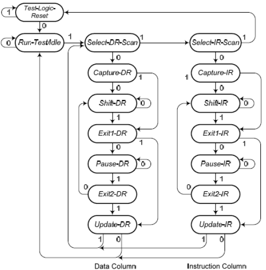
JTAG TAP controller statemachine
This state machine can be used to request the TAP controlled to talk to a device specific debug engine. This is illustrated in the figure below:
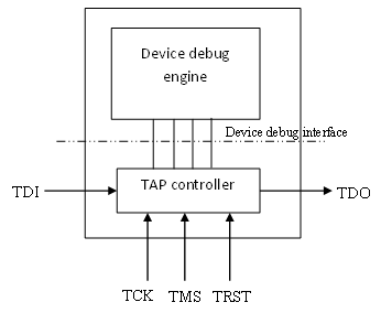
TAP and device debug interface
Examples of device debug engines include “EJTAG” in case of MIPS, “OCI” in case of some 8051s etc. They tie into the CPU logic to enable provisions like stepping through, PC redirection, instruction and data trace etc. We will later look into the specifics of one of these. For now, we will understand how JTAG can be used to communicate to these implementations in a generalized way.
To understand how JTAG TAP state-machine, operates, we need to first look into some more details of a generalized TAP pseudo implementation.
TAP controller contains an “Instruction Register (IR)” and one or more “Data Registers (DR)” that can be accessed over the 4-wire JTAG interface. At any given point in time of operation, the TAP controller will place one of these between the TDI and TDO lines. Data will be shifted into the register from TDI on the raising edge of TCK and data will be captured into TDO in the falling edge of TCK. So, to read data from a particular register between TDI and TDO, some dummy bits can be shifted into TDI that causes data present in the register to be pushed out via TDO.
TMS line is used to navigate the state-machine. State transition values shown in the state-machine are TMS values at the raising edge of TCK. So, for instance, to go into shift-IR state from Test-logic-reset, TMS should have the following values at the raising edges of subsequent TCKs : 01100 . Once the tap reaches shift-IR state, it will stay there as long as TMS is 0 . That means, TCK can be used for other purposes , without moving out of the state.
The state-machine is designed in such a way that holding TMS high for 5 subsequent raising edges of TCK will take it into “test-logic-reset” state irrespective of the current state. This is a quick escape hatch in case you screw-up :grimacing:
When the state-machine is in any of the IR states (like “shift-IR”, “capture-IR”, “update-IR” etc), the instruction register will be placed between TDI and TDO. Depending on the instruction pushed into the IR (and later captured), one of the data registers will be placed between TDI and TDO in the next DR state.
Length of the instruction register, binary encoding of an instruction and the instructions that are supported in a device are implementation dependent. However, certain instructions like IDCODE are recommended to be implemented on all devices. Implementation details are generally documented in the devices programming manual as well as in the device’s BSDL file. BSDL stands for boundary scan description language and is a subset of VHDL specification. Most JTAG based tools like Lauterbach Trace32 IDE has a provision to import a BSDL file and the instruction mnemonics can be used in a portable manner.
Assuming a 5 bit IR, and the binary encoding 00010 for IDCODE, placing the pattern in the TDI pin serially (LSB first) on subsequent raising edges of TCK while in shift-IR state will push in the IDCODE instruction into the IR that is between TDI and TDO in that state.
while in
Test-log-c-resetstate, device ID register will be the register placed between TDI and TDO in the next data phase.
While the last bit is being latched in, TMS need to be modified to go into capture-IR state. It is in this state that the TAP controlled decodes the instruction that has just been placed in IR. Next clock will push the state-machine out of capture-IR state into exit1-IR or “shift-IR” based on TMS state.
exit1-IRstate will terminate the scanning process and moving into subsequent states to reachcapture-IRfromshift-IRwill not alter the contents that were just shifted into IR
Once an instruction has been captured, the corresponding data register will be placed between TDI and TDO in the next “capture-DR” state. In this case, a data register containing the device identifier will be placed between TDI and TDO. So, once the TAP enters “capture-DR” state, contents of the ID register can be serially shifted out into TDO line at subsequent falling edges of TCK.
while the data register is being shifted out at falling edges of TCK, data in TDI will be shifted into the same register. So, assuming that TDI is held low during the process of reading out data via TDO, the register will end up with all
0s at the end of read.
MIPS debug subsystem
Since JTAG has a lot of implementation specific provisions, a specific processor family should be selected to understand how debugging (and programming) is achieved using JTAG.
For this study, we will be selecting MIPS32 family that has a debug subsystem named EJTAG that ties into the TAP and CPU debug features. The spec is available here.
EJTAG extensions and external virtual memory access
One of the primary features of MIPS with EJTAG extensions is its ability to virtually map the processors address space into the debugger. This essentially means that the processor will be able to execute instructions and process data coming from the debug probe instead of its own in-device memory (RAM/executable flash etc ). One of the ways to trigger this mode of operation is the EJTAGBOOT JTAG instruction that will cause the processor to reset and start accessing instructions from kseg3 that is virtually mapped into the TAP controller. (another mechanism is the SDBBP instruction).
Reset following EJTAGBOOT would would put the system in debug mode where all access restrictions are removed. The following bits in EJTAG Control Register (ECR) will be set following this reset.
- Debug Interrupt Exception Request bit (
EjtagBrk) indicating that a debug interrupt exception request is pending - Debug Exception Vector Control Location bit (
ProbTrap) indicating that the debug exception vector is at0xFF200200that falls within DMSEG region instead of0xBFC00480in normal boot case - Processor Access Service Control bit (
ProbeEn) indicating that the “probe” services processor accesses to DMSEG.
EJTAG control register is a 32 bit JTAG data registers that can be accessed using EJTAG
CONTROLinstruction)
Roccbit in ECR remains1following a reset until cleared by the probe. This is to force the probe to acknowledge a device reset. Until it is cleared,update-DRwill not update the control register.
CONTROL JTAG instruction will place the ECR between TDI and TDO for access in data phase of the TAP controller. When an EJTAG memory access is triggered following a debug reset with probe access the following is applicable:
PrAccbit in control register will be set to 1ADDRESSJTAG instruction can be used to shift out the 32-bit address that the CPU is trying to accessDATAJTAG instruction can be used to shift in/out the 32-bit data that the CPU is trying to read/writePszwill indicate size of data (0for byte through3for triple word)PRnWbit in control register will indicate whether it is a read (0) or write(1) operation pending on the address inADDRESSregister by the CPU.
CPU will be stalled until PrAcc bit is cleared . EJTAG probe (and debug software like the IDE) periodically polls the TAP control register for PrAcc and handles the request accordingly by shifting in/out data and clearing PrAcc once data access requested by CPU is ready.
This set of provisions lets the MIPS CPU execute instructions that are provided over JTAG. When this is used in conjunction with the CPU debug features that we will be seeing soon, a full fledged debugging system can be developed over the JTAG interface.
CPU stalls with
PrAcconly when access to dmseg addresses (starting at 0xFF20_0000) are made. So, for instance if an execution passed from the probe tries to access a RAM location, CPU will go ahead and fetch data from RAM and stall only for next instruction to be passed on via the probe (when PC starting at a DMSEG address is incremented by 1). In case of a jump to a non-dmseg address, CPU will jump to that location and continue execution and not stall until the next access to dmseg address is made.
CPU debug features
To enable extensive debug support, MIPS CPUs define a “debug” mode where the system enters a un-restricted access mode. dseg (where DMSEG and DRSEG resides) is active mapped only in this mode and this allows access to all hardware resources used for debugging as well as to all memory regions (Generally, some memory regions are accessible in kernel mode and not in user mode).
Debug mode is entered via a debug exception and the processor will be in debug mode when DM bit of CPU debug register is set to 1. DRET instruction makes the system exit from debug mode. DEPC register contains the PC address for return from debug exception
MIPS CoProcessor 0 (CP0) contains a Debug register (reg 23) that provides information about behavioural aspects of the system in debug mode. Only DM bit that shows current debug mode state and VER bit that shows EJTAG version are valid for read in non-debug mode. Other than the imprecise exception configuration bits, none of the other bits are writable in this register.
more details to follow


Leave a comment