

Building a RaspberryPi daughter card - warnings and pitfalls
This article has been migrated from my original post at embeddedinn.wordpress.com.
Raspberry Pi is a $35, credit card sized, single board computer that can run Linux and decode HD videos . There are many articles that describe how to bring up the board and play around with interfaces and GPIO. This article is for the DIY enthusiast who wants to extend the functionality of the “Pi” by building your own hardware around it.
I made a lot of silly mistakes wile I fabricated my first board at home. So, here I am sharing the experience I gained so that you wont repeat them in your trials.
Spec
The first problem I faced was my over-ambitious spec I had. Some of my key requirements where
- Single layer routing for toner transfer fabrication at home (being the first version).
- Small form-factor : even after attaching the card, I should be able to enclose the unit in its case.
- 28 pin pic micro controller running on a 20Mhz crystal oscillator with ICSP . [DIP package since that is all I had :smile: ]
- 2 user input switches, 3 LEDs, 1 potentiometer (A/D), SPI and UART connectivity for the µC
After spending 2 sleepless nights with eagle CAD free version, trying at least a hundred different placement combinations, manual and automated routing I realized the hard way that I have to admit defeat, or at least a partial one. All my specs can’t be met :weary: .
The constraints where:
- The final board size was predefined by requirement 2.
- Routing grid and clearance where defined by requirement 1. (especially by the toner transfer method that I chose )
These two made it impossible to accommodate all my peripherals. The saddest part is, I had enough experience and expertise in this kind of task and still I got excited and jumped ahead .
Finally I revised my spec to eliminate the pot and user switches and decided to provide the functionality from the μC.
The lesson: Do some analysis on paper to save time and hair :smile: . Patience is key to success
Placement
This daughter card had few specialties brought in by the fact that it is to be attached on top of an existing board. an initial mistake I made is not accounting for the irregular z-axis dimensions of components placed on the Pi. In the picture below, the yellow on black thatched area shows the clearance that is actually available on my board.
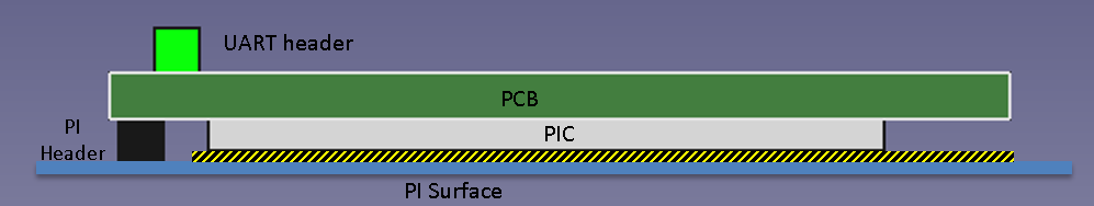
Diagram created in a combination of FreeCad and MS Word
While designing your boards, keeping track of the clearance after placement is critical for the final board to sit snugly on the Pi. I had to move the PIC a bit to the right to accommodate the power trans that stands proud on the component line. Using a vero-board to simulate the placement of components will be a fruitful exercise.
The lesson: A vero-board is your friend to simulate component clearence
Orientation
My board had some of the “user-passive” components like teh PIC placed under the board [i.e the component side], while the “user-active” components like LEDs and reset switch placed on trace side of my single layer board. [The LEDs and switches where SMD packages] This presents a challenge in the placement orientation of the components for a single layered toner transfer design.
In case where there is a mixture of I generally do all my rouging in the top layer (red). Once this is decided, I place all my SMD components “as-is” [No flipping, no turning]. Then I placed the 2×13 row header [i used a con-harting 13] that connects to the Pi. This had to be flipped as seen in the image below so that the connector aligns properly when inserted.
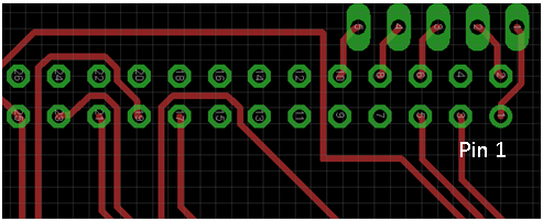
The PIC part could be placed as such since the flip orientation is automatically taken care of.
Using the “set pad_names on” command in eagle is very useful in these scenarios.
The lesson: Visualization is key to orientation success.
Pads
As you can see in the header picture above, the pads are very thin. Working with this type of pads in toner transfer method and hand soldering is a nightmare . Having to hand drill the pad holes makes things even more challenging. The easiest way to overcome this is to edit the parts to suite our requirement. This is much more easier than designing parts from scratch.
To edit a part, right click on the aprt and select open package. Then make the required changes, save and replace the existing part with the new part. The diagram below shows a partially edited part
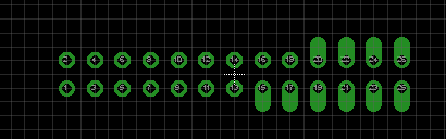
The lesson: understand your design constraints and re-use existing parts to suite your needs.
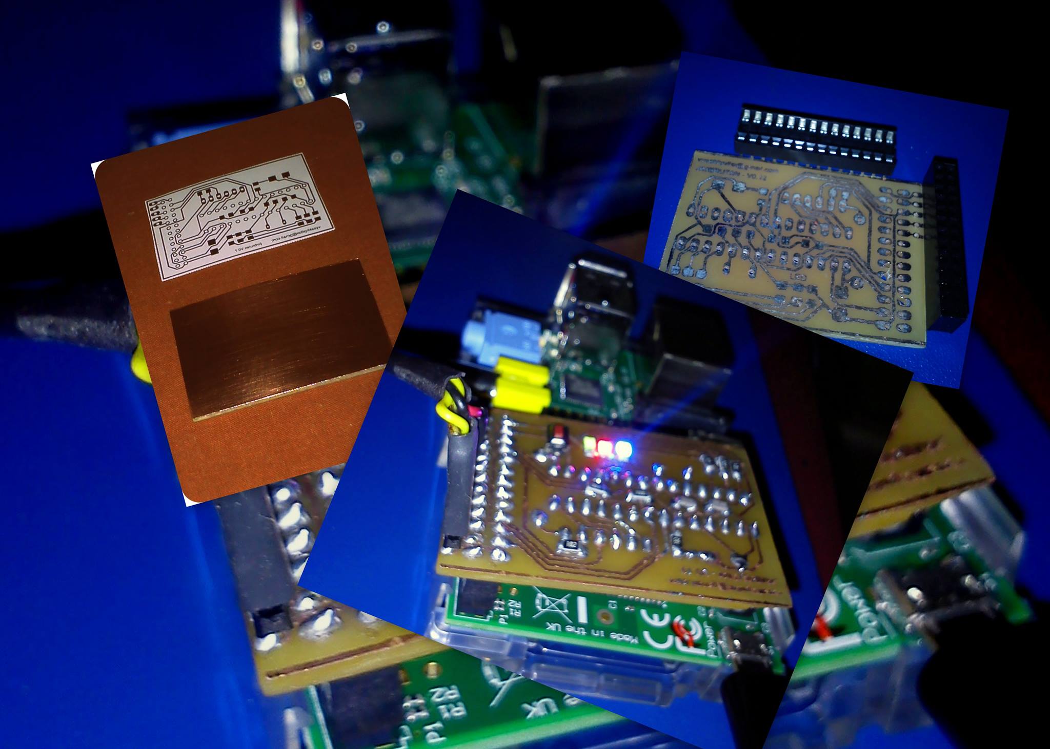
My Board
This is a pic of my final board


Leave a comment