

PIC microcontrollers
NOTE: The IDE used in this article has been phased out by Microchip. However, basic techniques and architecture described herein holds good.
The first instance of this article originated at my google site page. It was further migrated to wordpress and then this page.
INTRODUCTION TO MICRO-CONTROLLERS
A micro-controller, in simple words, is a miniature computer with a central processing unit and some peripherals integrated into a single integrated circuit package.
The central processing unit can can execute some instructions resulting in some outcomes. This instructions define the architecture of the controllers central processor in a macro scale.This gives rise to the a major classifications in processor architecture as
- Reduced Instruction Set Computer (RISC)
- Complex Instruction Set Computer (CISC)
To learn about controllers, processors and architectures in a general and abstract manner is tedious, time consuming and at-times dry. So here we are considering a simple microcontroller – the PIC 16F877a as an example to begin with.
PIC 16F877a is a mid range microcontroller from microchip inc. It is a CMOS FLASH-based 8-bit microcontroller with a RISC architecture that can handle 35 instructions.
When studying any electronic device or part, the bible is its datasheet. The data sheet describes in detail the architecture, capabilities and requirements of the part. PIC16F877a ‘s datasheet can be found here.
Download it and keep it for further reference throughout the tutorial. A printout of section 15 of the datasheet (only 6 pages) will be a great help during the programming exercises.
Getting Started
As said in the introduction, PIC micro controller, like any other micro controller executes the instructions one at a time in a sequential order as stored in its program memory and it is the skill of the developer to use these instructions (35 in this case) to create magics (like an intelligent robot). The programs written using these basic instructions are called assembly language programs and is the most primitive (not exactly, but close [:D]) and optimized form of programming.
An assembly language program will look something like the snippet given below
movlw 0xfa movwf 0x20 movlw 0xdf addwf ox20,1
The above snippet is to add two numbers and does what the algorithm below does.
x=250; x=x+223;
The second form is easier to understand and manipulate from a programmers point of view. But to learn the architecture and functionality of the micro controller, we have to deal with the assembly language programming. Since it gives a clear cut idea as to what is happening inside the device – i.e. the data flow within the device and which internal modules are involved, we can also optimize our code for best performance.
Now, to get started with, we need two things.
A software that can simulate the internal working of the PIC micro controller and the datasheet of the device.
MPLAB IDE from microchip to simulate the device. MPLAB Integrated Development Environment (IDE) is a free, integrated toolset for the development of embedded applications employing Microchip’s PIC® and dsPIC® microcontrollers. The latest version can be downloaded for free here.
We will be using this software to simulate instruction flow within the PIC microcontroller and there by understand its architecture.
The data sheet is the document in which the device vendor release with the product. It will have all the device details and specifications for end users. Once we are familiar with the basic concepts of microcontrollers, we can explore the data sheet on our own and discover newer tricks. The datasheet of PIC 16f877a can be downloaded from here.
Architecture – A general Introduction
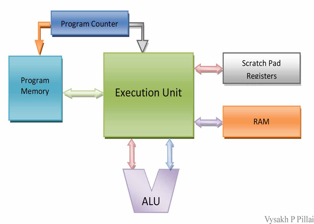
General Processor Architecture
Shown above is a simplified processor architecture. ( A more proper ‘Processor Architecture’ is to indicate the memory connectors as buses since most processors maintain an external program and data memory, while controllers have them in-built along with other peripherals. But, I want to keep the picture simple so that explanation will be easier :smile: ).
The firmware (program) resides in the program memory. Once the processor is reset and ready to go, the program counter, which is simply a counter that acts as a pointer to the program instructions points to the initial location of the program memory.
The execution unit fetches the program instruction in this first location. This will be one of the 35 instructions that the PIC can handle in our case. These instructions are stored in the program memory in an encoded fashion. It will be a binary number that has encoded information relevant to the instruction.
For example, the instruction movlw 0xff will be encoded as 11 0000 11111111 when stored in the PIC 16f877a program memory. This 14 bit encoded binary contains the instruction, the scratch pad memory location to be used and the literal value 0xff. A complete list of instructions and their encoding is given in page 160 of the datasheet.
The task of the execution unit, in simple words, is to fetch the instructions pointed to by the program counter (PC), understand it (Decode) and execute it.
Execution of a command can include a wide variety of tasks like moving some data from one RAM location to another, or storing it in a non-volatile EEPROM location, or communicating with an external device like a PC. These tasks vary from micro controller to micro controller. A user side view of these tasks can be obtained by analyzing the instruction set of the specific device we are planning to use.
RAM is the volatile memory integrated within the controller package. It provides working space for the data manipulation during the command execution. The amount of RAM available is an important metric as the speed of operation and instruction set for a micro controller.
Scratch pad memory registers are high speed memory registers which are integral to the processing center architecture. The concept is from processor architecture, since the external memory access which will be much slower can be a bottleneck to the high speed operations within the processor. Microcontrollers usually have one or two such registers only.
PIC Architecture
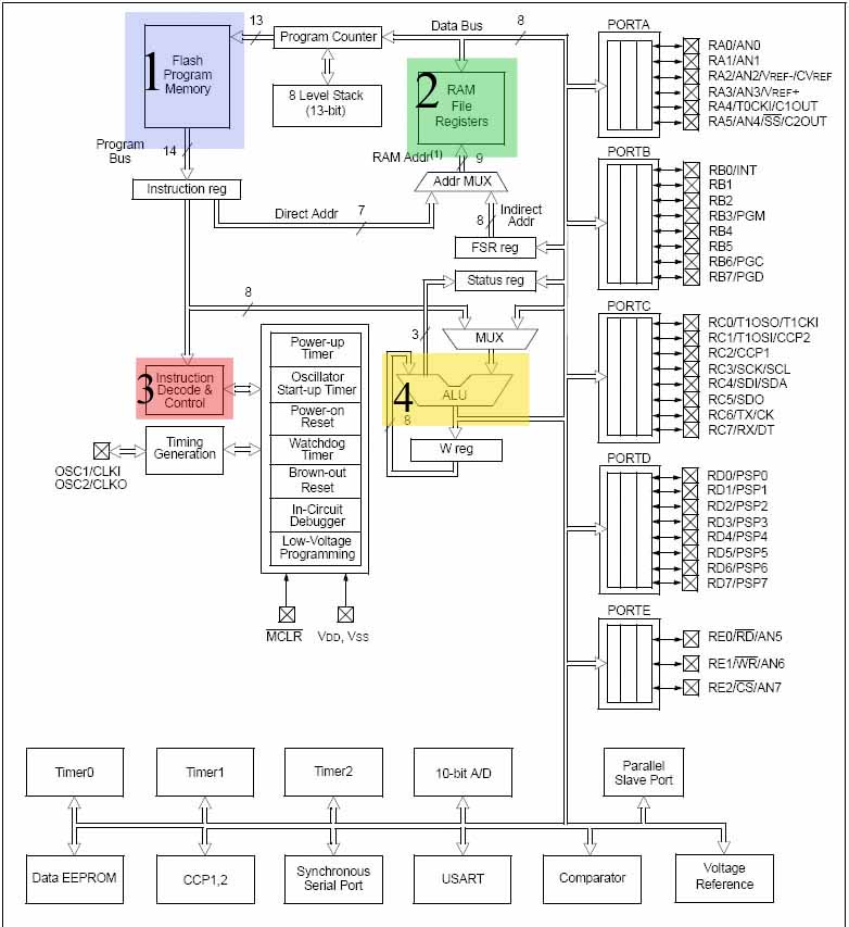
PIC16f877a Architecture
Based on the memory organization, processor architectures can be divided into two as
- Von Neumann Architecture and
- Havard Architecture
Our point of interest here is that the Von Neumann architecture has a common bus for program memory and data memory (RAM), where as the Havard architecture maintains separate buses.
PIC 16F877a has the havard architecture, as it can be noticed from the architecture diagram above.
We will analyze the architecture in light of the general introduction in the previous section. The blocks are identified below.
- Section marked 1 (blue) is the program memory.
- Section marked 2 (green) is the Data Memory (RAM).
- Section marked 3 (red) is the Execution Unit.
- Section marked 4 (yellow) is the ALU.
The instructions are encoded and stored in the non-volatile Flash Program memory. Upon reset, the program counter points to memory location 0x00. This point is the reset vector and contains the first instruction of the steps that are to be done once the controller is reset. Details of the actual reset mechanism and other details will be dealt with later on.
Under regular circumstances, the program counter increments by one every execution cycle (explained later, as of now, consider it as each clock). This new location is used by the execution unit to fetch the next instruction.
When the execution unit receive jump or loop instructions, it stores the current program counter value to the stack and loads the new program location to go to into the PC. Thus these instructions take two execution cycles to complete. (A complete listing of the execution times can be found in page 160 of the data sheet).
The stack has 8 levels. i.e the PIC can perform upto 8 jump instructions after which it can return to the original location without errors in execution.
A detailed explanation if the instruction set will follow later on in the tutorial, but for easy understanding of many of the concepts, it is advised to thoroughly go through the instruction set summary given in section 15 of the datasheet (6pages) before proceeding further.
Let us consider an example to make this clear.
00    movlw 0xf0              ; moving value 0xf0 to location 0x22 through w register
01    movwf 0x22
02    call rtn1               ; a jump instruction to label rtn1, pushes 03 (next PC)
                                           ; to stack and loads 05 (rtn1) to PC
03    movfw 0x24              ;moving value in location 0x24 to location 0x23 through
                                           ;w register
04    movwf 0x23
05    rtn1:   movlw 0x8f      ;moving value 0x8f to location 0x24 in data
06                 movwf 0x24             ; memory
07                 call rtn2  ;pushes 08 to stack and loads 11 to PC.
08                 movlw 0xa0 ;moving value 0xa0 to location 0x24
09                 addwf 0x24 ;adding the value 0xa0 to content of
                                           ;location 0x24
10    return                  ;pops 03 from stack and loads to PC
11    rtn2:     movfw 0x24    ;moving content of location 0x24 to location 0x25
                                           ;through w register
12                  movwf 0x25
13                  return    ; pops 08 from stack and loads it to to PC
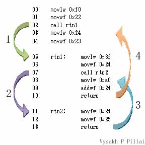
In the above code snippet, the PC increments by one until the execution unit receives the call instruction at 02. Once it receives the call, the immediate next location address (03 here) is ‘pushed’ (stored at the top most level) into the stack and the destination location (05) is decoded form the instruction and is loaded into the PC. Thus , at the next execution cycle, the instruction fetched is the movlw at 05. Then the regular operation take place with the PC increment from 05.
At 07, another call instruction is encountered. Again, the immediate next PC (08) is pushed into the stack. this makes the previously stored 03 to go to the second level of the stack and 08 recedes in the first level.
At 13, a return instruction is received this causes the first level of stack (storing 08) to ‘pop’ the topmost level into the PC. So, now the PC points to 08. Normal execution continues till 10 where the return instruction pops 03 from the stack.
Here we utilized two levels of the stack. If there are more than 8 consicutive ‘call’s without return, the first pushed data will be over written. This will corrupt the firmware. In those cases, we have to develop routines for stacking.
PIC memory map
Operations resulting from the execution of instructions can all be considered as manipulation of data in different parts of the micro controller. It may be data in the RAM or in other special registers with designated purpose. These special registers (Special Function Registers (SFRs)) also reside within the RAM register block, but cannot all be manipulated like ordinary memory registers, without ‘side effects’.
The RAM block (512 bytes in size) is not one single continuous block of memory, but is rather divided into four banks of 128 bytes each. Of this, 368 bytes are General Purpose Registers (GPRs) and the remaining 56 are SFRs. The distribution of this GPRs and SFRs in the RAM register block can be seen in page 17 of the datasheet. The location of each of the SFRs and the range of the GPSs in each bank is clearly shown there.
Data cannot directly be written into or transferred from one RAM register to another using any of the 35 available instructions. rather, it has to be transferred via the scratchpad registers. Before the transfer the appropriate bank is also to be selected.
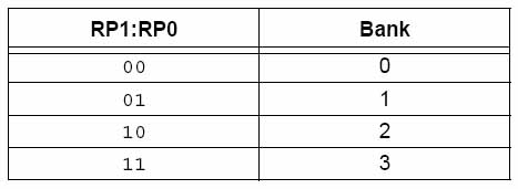
Bank selection is done by writing the appropriate values into the bank selection bits of the STATUS register. ‘STATUS’ is an 8bit SFR available in all the four banks. The 6th and the 5th bits of the STATUS register are named RP0 and RP1 and is responsible for selecting the current bank. The table of selection values is given below.
The working register, commonly referred to as the W reg, is the only scratchpad memory register accessible to the user in the PIC 16F877a. It resides outside the RAM register block. Every data transfer in or out of the RAM register has to go through the W reg.
For example, if we want to store the value 0xff (Hexadecimal of 127) into the GPR located at 0x20, we have to first transfer the value 0xff (literal) to the W reg, and then transfer the value to the register location (refered to as ‘file location’) 0x20 in another instruction. The code for the same will look like this.
bcf STATUS,RP0  ; Clear(set to 0) bit RP0 of the file register
                                ;STATUS for bank selection.
bcf STATUS,RP1  ; Clear(set to 0) bit RP1 of the file register
                                ;STATUS for bank selection.
movlw 0xff      ; move literal value 0xff to w
movwf 0x20      ; move value in w to file location
                ;(register) 0x20
Once this is done, the value remains in the location until either it is changed by another instruction or the micro controller is reset or powered off.
Execution Cycle
A microcontroller is a synchronous digital device.i.e. it works based on the timing pulse recived from the systems clock circuit. The PIC 16f877a can generate its own clock from a piezo crystal connected to its specific pins.(This is the most popular method of clock generation for its accuracy. Other methods are also available, which will be discussed later).This crystal can be up to a maximum speed of 20Mhz. But, this doesn’t mean that the PIC can execute instruction at a maximum speed of 20,000,000 instructions per second (50ns per instruction).
The clocking signal derived from the crystal is internally divided by four. This is to provide synchronization timing and clock signals to all parts of the micro controller. However, the division of master clock is primarily to establish an instruction pipeline. Thus, if we generate a 20Mhz master clock, the execution speed will be a maximum of 5Mhz. The single cycle instructions execute at this speed.
We can get a better idea of pipelining by considering the famous laundry example.
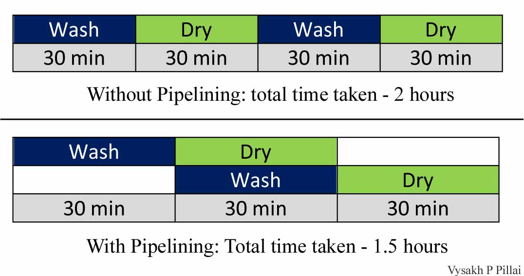
Consider a laundry with one washing and one drying machine. If operations are carried out one after another, the entire task (to complete two sets of laundry) takes 2 hours. This is like fetching, decoding and executing instructions only once the previous instruction is completely finished.
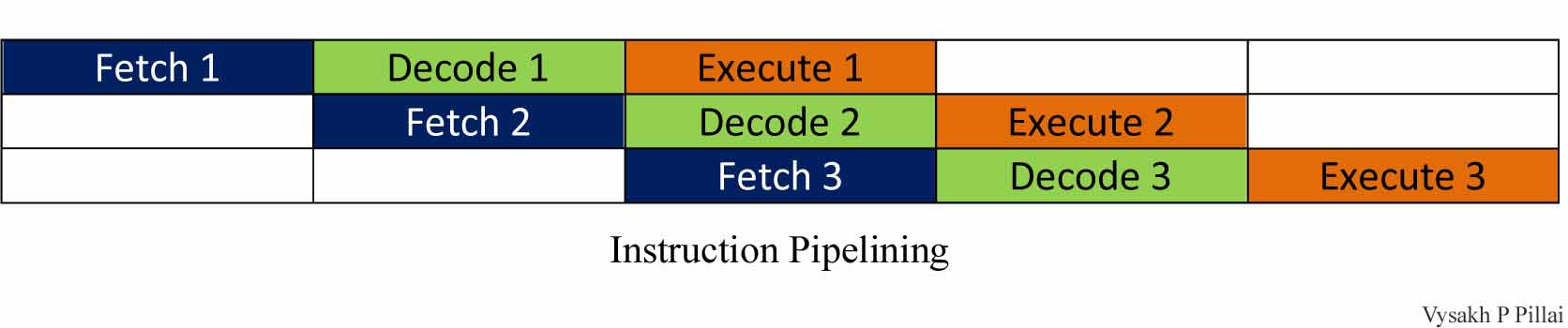
But, while the first set is being dried, if the second set is put to wash, the operations are carried out parallel, thereby saving net time. This is the case of instruction execution with pipelining. When one instruction is being executed, the next instruction is fetched and decoded, making it ready for execution. This is illustrated below
Ports
A port is the microcontrllers’ interface into the real world. All the data manipulation and operations that are done within the microcontroller ultimately manifests as output signals through the ports.
To make the concept clear, let us consider an air conditioning system built around a microcontroller. The temperature sensors measure the room temperature and gives it as input to the microcontroller through the ports. The data coming in through the ports will be stored in some GPR by the microcontroler. The data in this GPR will be compared against a set temperature. If the external temperature reported by the sensor is higher that the threshold, the microcontroller switches on the air conditioning mechanism. This is done by switching on the corresponding port pin.
Physically, ports are some of the pins that are seen in the IC package. There are 6 ports for PIC 16f877a. They are named as PORTA, PORTB, PORTC, PORTD and PORTE. Ports B, C and D are 8 bit wide (8 pins each), while PORTA is 5bitand PORTE is 3 bit wide. The pin allocation of the ports are given in the IC pin diagram in page 3 of the data sheet and is reproduced below. The individual port pins are named 0 throug n. for eg 1st pin of PORTA will be RA0.
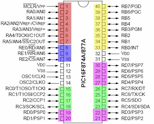
As it can be seen from the pin diagram, the port pins are bi-directional and and most of them are multiplexed in function. i.e the pins act as regular general purpose I/O as required for the air conditioning example, or as the I/O s of some of the internal modules of the microcontroller. For example, port pins RC7 and RC6 (pin number 25 and 26) are regular I/Os as well as the interface to the UART module that handles the RS-232 protocol, which is commonly used to interface the PIC to a regular computer.
The RS-232 based UART module requires only two data lines to effectively transmit and recieve data from a regular computer to the PIC or even a printer or PDA with a serial port. This module is integrated into the PIC package and can be configured using firmware instructions. Exact way of doing this will be discussed later.
Each port has a corresponding SFR in the RAM register block. Therefore , when we are referring to switching a port pin on as in tha air conditioner, it is actually writing data into the corresponding port register. Similarly, receiving data from the registers is actually, reading the data stored in the corresponding data register.
Along with the data holding port registers, there is a set of configuration registers associated with the ports. These are the TRIS registers that configure the ports to be in input or output mode. These also reside in the RAM register banks as SFRs. Writing a 1 into the corresponding TRIS bit configure the port pin as an input pin, and the data comming in throught the port pin will be latched into the corresponding PORT bit in the immediatly next execution cycle.
The code snippet below is to read a byte from PORTB and write it to file location 0x120. Note that the TRIS registers are in bank1 where as the PORT registers are in bank 0 and file register 0x120 is in bank 2. This bank selection concept is to be kept in mind whenever we are dealing with RAM registers of the PIC. The list bank location listing is in page 17 of the data sheet.
bsf STATUS,RP0    ;Selecting BANK 1 for TRISB register
bcf STATUS,RP1
movlw 0xff        ;Moving the 1s (since PORTB is to be set
                   ;as input port) to be stored at TRISB to w reg
movwf TRISB       ;moving the 1s to TRISB
bcf STATUS,RP0    ; Selecting Bank 0 for PORTB
movfw PORTB       ;Moving Input at PORTB to w reg to later move to 0x120
bsf STATUS,RP1    ; selecting BANK 2 for 0x120
movwf 0x120       ; moving valiw in w reg from PORTB to 0x120
Note that the port pins can also be individually configured, i.e. any combination of input and output configuration is possible in any of the ports.
Instruction Set
The key architectural concepts of the PIC 16f877a microcontroller has been discussed. Now, we are going into the actual program writing process. Some of the instructions like MOVWF and MOVLW should already be familiar to you since it has been used over and over again in most of the examples already discussed. I hope you have also gone through the instruction set summary (Section 15 of datasheet) as instructed. If not , this is the point of time to do so. Go through the explanation of each and every instruction.
An instruction set is the entire set of commands that a microcontroller/processor can execute. Any task to be accomplished with the device is to be split up and written in terms of the defined instruction set. For example, if multiplication of two numbers is to be performed in PIC 16F877a , there is no direct instruction to do it. This is because the ALU of the microcontroler has no provision to do it. Therefore , if we have to do the multiplication, we have to write a routine out of the available looping, counting and addition instructions that are available.
Writing routines in the native instruction set is called assembly language programming. This method will give the most optimized firmware, but required a great deal of skill and is hard to debug, especially as the system size grows and advanced concepts like multi-tasking, resource sharing etc comes into picture. However, assembly language programming is the most effecient way of learning the architecture of the system and is also fun.
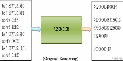
The programs written in the assembly language is further to be converted into binary encoded format so as to use it in the microcontroller. This is dome by the assembler software. Most of the device vendors provide a free asembler for their parts. So is the case with microchip. The MPASM software that converts assembly language programs into binary .hex files usable by the controller.
A simulator is a software that simulates the working of the device in detail. Using a simulator, we can simulate the loading of a program, execute it step by step, analyze the effect of each instructions in different registers of the controller and thereby debug and fine-tune the firmware. MPLAB IDE is the integrated development environment provided by microchip, which can assemble our firmware and also simulate it. It is available for download, free of cost from here.
detailed explanation of how the assembler works can be found here.
We will be using the MPLAB IDE to explore the instruction set, and observe the results.
Since a very detailed explanation about the instructions is available in the datasheet, we will be focusing more on how to get things done using the 35 instructions. This will be mainly my taking simple examples and running it in the simulator in the initial stage and later on using the hardware itself.
MPLAB IDE
Before beginning the actual coding and analysis, let us familiarize with the simulator – MPLAB IDE.
We will be dealing each example as a different ‘Project’. It is the IDE’s way of handling all the associated files like the assembly file, the hex file etc as a single virtual entity. It is also easier for us to keep track of our files this way.
Once the IDE is initialized (opened), to begin a project, go to project - ‘project wizard’ from the task bar.
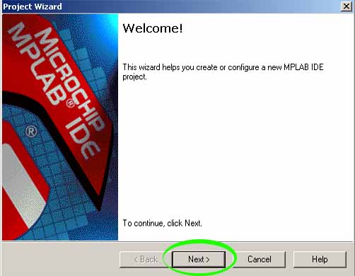
Click Next…
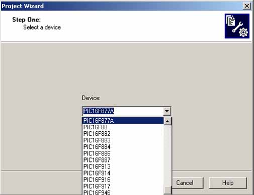
Select the device (PIC16F877A) from the drop down list and click next.
The IDE is an environment which integrates different simulation tools and compilers to provide a single window solution to development and debugging.
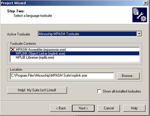
Here, we have to select the toolsuite (Microchip MPASM Toolsuite) which include the assembler, the linker and the libraries. the tool suite components resides in the ‘MPASM Suite’ folder within the installation folder. In case any of the components are not correctly pointed correctly, a red cross mark appears near the component. browse to the location the remove the indication before continuing.
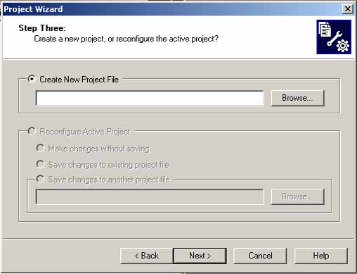
Now, browse to the location where the project files are to be stored and give your project a name. Note here that if the full project location name length is greater than 62 characters, then the assembler will show error during the linking process. Keep that in mind while choosing the project name and location.
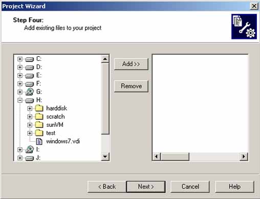
If the assembly or some other relevant files like libraries that are to be added to the project already exist, then add it here. 1st timers can skip this step…
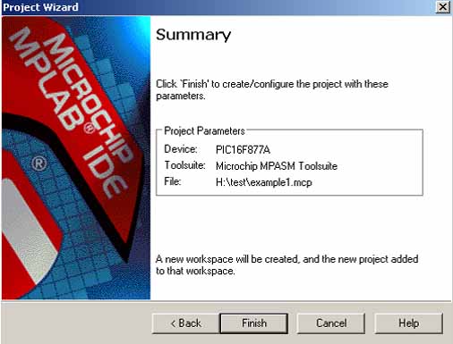
Now we have successfully created our project and a summary will be generated.
Now create a new editor file by going to file - new (ctrl+n). This is where we will be entering our code. To activate the colour coding that will highlight keywords, type in something and save the file with the .asm extension to the project folder.
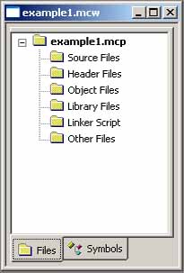
Once this is done, we have to add the file to the project. For this first activate the project view by clicking view - project. This will add the following screen to the workspace. Right click on the ‘Source files’ and click ‘Add Files…’
Browse to the assembly file we saved before and click add.
Next step is to define the simulator that we will be using. for this go to Debugger - Select tools> and select MPLAB SIM
Now we are all set to go coding. We will start with some examples and later go into building intelligent machines :smile: .
Hello World
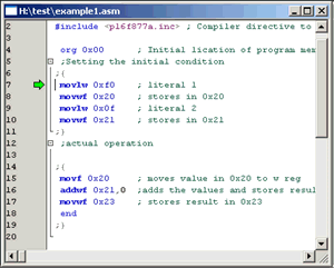
This is our first program that we will be simulating using MPLAB IDE. This will be to add two numbers and store the value in a file register. To keep things simple, there will be no user input, rather the literals to be added will be stored within the micro-controller and so will be the result.
Problem Statement
Two values stored in file register locations 0x20 and 0x21 are to be added and the result stored in register 0x23.
Code
list p=16f877a                        ; compiler directive to set the device used
#include <p16f877a.inc> ; Compiler directive to include library

org 0x00      ; Initial location of program memory

;Setting the initial condition
bcf STATUS,RP0 ;setting bank 0
bcf STATUS,RP1
movlw 0xf0     ; literal 1
movwf 0x20    ; stores in 0x20
movlw 0x0f     ; literal 2
movwf 0x21    ; stores in 0x21

;actual operation

movf 0x20        ; moves value in 0x20 to w reg
addwf 0x21,0   ;adds the values and stores result in w reg
movwf 0x23     ; stores result in 0x23
end
Now, we are ready to start the simulation and watch the internal operations of the microcontroller.
Note: The device library p16f877a.inc contains the SFR name to address mapping. It is included so that we can use the register names like STATUS and RP0 instead of having to give in their address each time. Writing code as bcf STATUS,RP0 is easier than writing bcf 0x03,5 since we’ll have to remember the addresses of all the SFRs and debugging will be tough.
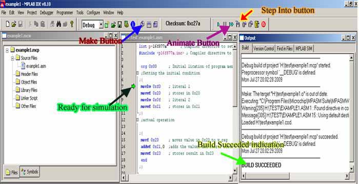
Compilation (make)
Once the code is entered, it needs to be compiled . Compilation invokes the assembler and generates the hex file. It also checks for syntax other possible errors during the process.
To compile the code click the ‘make’ button in the tool bar.
Workspace
Simulation
Before actually beginning the simulation, there are a couple of settings to be made.
- Switch off the device watchdog timer by going to configure - configuration bits (The reason will be explained later on)
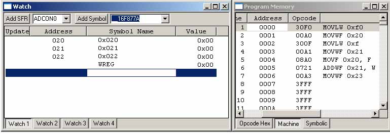
- Enable the Watch window and program memory window by going to view
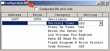
To switch off the watchdog timer, uncheck the configuration bits set in code check box indicated in the figure and select the option from the drop down menu.
In the watch window, add the relevant register names by double clicking under the corresponding tab (Adddress/ Symbol name) and typing it in or in the case of SFRs, selecting it from the ‘AddSFR’ drop down.
The Program memory window gives us an idea as to where our program is residing in the program memory. It will be interesting to note this change in location by Changing the ‘org 0x00’ line to some other locations like say, ‘org 0x20’. But corresponding lines will have to be added at the reset vector (0x00) for successful execution. the next example will demonstrate that.
Now we are ready to run our simulation. The required buttons are shown in the workspace figure.
Click on the ‘step into’ button to execute each instruction sequentially. The green arrow shows the current execution that has been decoded and ready for execution. The corresponding trace of the program memory location can also be seen in the program memory window. The resulting change of values in the registers after each operation can be noticed in the watch window. Once the execution reaches the end statement, the program fetch and decode continues and can be noticed in the PM window, but the instructions are all NOPs. however, leaving the controller to blindly execute instructions in unhealthy practice, and the control should be rightly directed using CALL or GOTO operations.
The reset button can be used to regain the control to the reset vector .
Note: Each click to the ‘step into’ button can be considered to be generating a pulse of the execution clock.
Simulator Tweaks
After the first program, we are now all set to try out more interesting stuff. I’ve introduced the basic simulation technique in the previous ‘Hello World’ page. Let us explore some more cool features of the simulator, that will allow us to further explore the architecture and functionality of the device.
These sections introduce the simulator as well as the coding styles. So pay attention to the codes and comments…
Animation
In the previous example, we ran the simulation by manually clicking the ‘Step Into’ button to execute each instruction. This is like manually providing the execution cycle clock for each instruction. In realtime, the execution clock is automatically generated from the crystal and is continuous. This can be simulated using the animate button.
Before jumping into the implementation, a couple of settings are to be made so that we can observe the animation sequence.
Go to debugger>settings .
In the Osc/Trace tab set processor frequency as 4Mhz. (We are using it so that it’ll comply with the hardware experiments later)
In the Animation/Realtime updates tab set, set animate step time as 500ms and check the ‘enable realtime watch updates’ check box and set the value to 5 (x100) ms.
The later step is to keep the animation steps visible. otherwise, the animation will be too fast for us to see. (The snapshot in the ‘Hello World’ page is running with these settings. (see it here)). The animate step time of 500ms is the execution frequency for the simulation (only!).
Simulator Logic Analyzer
The simulator logic analyzer tool is a very handy tool that gives the feel of the familiar oscilloscope interface. The following example of generating a square wave in RB0 shows a rookie level example of how cool this tool is.
The tool is available at View>Simulator Logic Analyzer
Problem Statement
Generate a square wave of 50% duty cycle at RB0. and verify the output using the Simulator Logic Analyzer.
Code
list p = 16f 877a ; compiler directive to set the device used
#include <p16f 877a.inc> ; Compiler directive to include library
org 0x 00 ; Initial location of program memory
goto start ; instruction at PM location 0x 00

org 0x20
start ; label marking PM location 0x 20
  banksel TRISB;a compiler directive that eases
                ;the bank selection job
  movlw 0x00
  movwf TRISB ;setting PORTB as output port
  banksel PORTB

loop ;infinite loop generating the SQW
  bcfPORTB,0
  call delay ;used to set the time period
  bsf PORTB,0
  call delay
  goto loop

delay  ;This code segment counts down from 255 to 0
       ;each count takes up some time thus
;generating a delay loop
  banksel 0x20;bank selection
  movlw 0xff ; initial value
  movwf 0x20 ;count register

decloop ; The decrement loop
  decfsz 0x20 ;decrement 0x20, skip next instruction is value in
;0x20 is 0
  goto decloop ; executes if value in 0x20 is not 0
  return   ; executes when value in 0x20 is 0.
end
Notes:
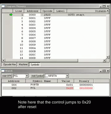
- Note here that at reset, the control jumps to
0x20since it is the instruction at the reset vector - When Delay is called, the next PM value (
0x0028) is pushed into the stack and the PC is loaded with0x2D - When return is called, the Stack is popped. This can be observed in the hardware stack window.
The Delay: Delay routines are generated usually using timers inside the controller. here, we are using a decremental counter. The decrement operation takes one execution cycle per operation. i.e. once the control enters the routine , it takes 256 execution times to pop the stack. When converted to time, it will be a delay of (256x1us) assuming a oscillator frequency of 4Mhz.
Result
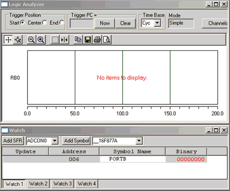
The animation result as seen in the logic analyzer is shown in fast forward here. Without the tool, we will have to visualize the square wave from the alternating ones and zeros in the watch window. This is also shown in the image.
The binary view can be availed by right-clicking within the watch window and selecting the corresponding option.
Breakpoints and the Run button…
When we where dealing with the delay routine, you would have noticed that the execution time of the instructions in the animation mode is equal to the animate step time we have set in the debugger options and not the actual time the microcontroller takes in the field. This is rather annoying when we have to run the entire sequence (code) for a while to see say, 10 square waves in the logic analyzer, since the operations are in “slow motion”. Also, the time period of the square wave is not what the original hardware would produce.

To solve this problem, we use the concept of breakpoints and the ‘Run’ button.
Problem statement
Generate a 10 second (real time) delay using delay loops.
Code
list p=16f877a ; compiler directive to set the device used
#include <p16f877a.inc> ; Compiler directive to include library
org 0x 00 ; Initial location of program memory
goto start ; instruction at PM location 0x 00
org 0x20
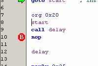
start
calldelay ; Calling the delay loop
nop ; Breakpoint is set here
delay ;This is a 3 level
cascadeof our previous delay loop
movlw 0x 35 ;value 1
movwf 0x 22 ;Total = 53 x 256 x 256 x 256
loop6
decfsz 0x22
gotoloop1
gotoend1
loop1
movlw 0xff ;Value 2
movwf 0x21
loop4
decfsz 0x21
gotoloop2
gotoloop6
loop2
movlw 0xff ;Value 3
movwf 0x20
loop3
decfsz 0x20 ;Innermost loop
gotoloop3
gotoloop4
end1
return
end
The functionality is somewhat self explanatory 3 level cascade of the previous delay loop. It can also be observed using the simulator for clarification.
Our primary aim is to measure the amount of delay this loop can give us.
The Run button executes the command eliminating the visual effects we get from the animation. But we need to have a control as to in which step of the execution, we need to pause to read out the register values from the watch window. For this, we use the concept of breakpoints.
To set a breakpoint, double click in the grey area near the line we need to breakpoint. The breakpoint symbol will appear. The execution pauses when it reaches this step. We can use this pause to make required readings and continue with the simulation.
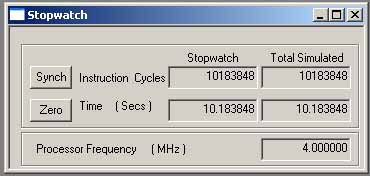
Now, to simulate real-time execution data, we have to use the ‘Stopwatch’ feature in the Debugger> menu. The readings it shows is dependent on the processor frequency that has been set in the Debuggre>settings>Osc/Trace tab. This is the crystal frequency we anticipate to implement in hardware.
Now, let us find out how much delay our routine can give us…
Set the breakpoint near the nop in line 10, and hit the run button.
The entire routine will be executed and the execution halts at the breakpoint. the exact time taken to execute the routine viz our delay will be shown in the stopwatch…
To change the delay value, experiment changing the different seed values indicated in the comments.


Leave a comment